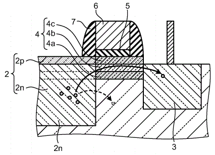
Toshiba patent application US20150008482 "Semiconductor device and manufacturing method thereof" by Motoyuki Sato says that making SiGe superlattice under transfer gate can drastically reduce the influence of SiO2/Si interface traps that potentially can capture photoelectrons during the transfer. The dark current and white pixel defects are also said to be reduced:


Tidak ada komentar:
Posting Komentar